 |
|
|
| Mass and Volume | 480 gm, 6 X 8 X 12 cm |
| Power | 3.5 W imaging |
| Optics | 9-element refractive |
| FOV | 65.9 degrees |
| IFOV | 1.25 mrad (7.5 m @ 6 km, 12.5 cm @ 100 m altitude) |
| f/ratio | f/5.6 |
| Focal length | 65.9 degrees |
| Detector | Kodak KAI-1001: 1024 X 1024 (1018 X 1008 photoactive), 9 Ám pixels, 20% fill factor, interline transfer electronic shuttering |
| Noise | 50 e- |
| Full-well | 40,000 e- |
| Exposure Time | 4 msec |
| SNR | 60:1 (albedo 0.1, i = 70 degrees) |
| Bandpass | Panchromatic |
| Electronics | Four surface mount assembly printed circuit boards connected by flexible circuit board cables |
| Microprocessor | Motorola DSP 56166 @ 60 MHz, 4096 Bytes Program RAM, 4096 Bytes Data RAM |
| Communications | Synchronous port @ 1 Mbps/port Signals: RS-422 receive, transmit, clock, frame synch |
| Frame Time | 0.5 sec for heatshield jettison, 5.3 sec during parachute descent, 4.0 sec during powered descent |
| Digitization/Compression | 12-bit ADC, Square Root encoded to 8 bits 1.8:1 lossless Huffman first-difference (realtime in DSP) |
| Data Return | up to 30 images: four 256x256 of heatshield jettison, sixteen 1024x1024 circularly-edited during parachute descent, ten 800x800 during powered descent |
Optics
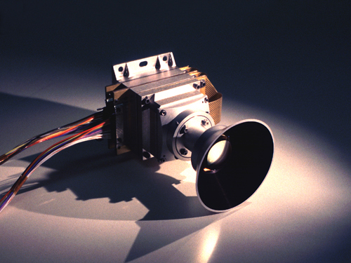
The MARDI optics provide a nominal field of view (FOV) of 65.9 degrees (1) across the 9 mm square photoactive area of the CCD. The lens has an effective focal length of 7.01 mm, a focal ratio of f/5.6, and weighs approximately 100 gm.
The systems has 9 elements, including two cemented doublets. All optical surfaces are spheres except for a weak asphere immediately after the aperture stop, which deviates less than 3 waves at 633 nm from spherical. The optical performance properties are weighted for martian spectral radiance in the 500 nm to 800 nm band, although no bandpass filter is included in the optical path. The lens is designed to provide high modulation transfer function (MTF) performance over the entire field. Testing of the flight optics at 633 nm showed an MTF at the Nyquist frequency of the detector (56 line pairs per mm) of approximately 80%, even at the edges of the field. The broadband performance is somewhat lower.
The lens barrel and sun shade are made of anodized aluminum. The design is athermalized to maintain focus over the expected temperature range. The optics are approximately 3.7 cm in diameter, including the sun-shade. When integrated with the MARDI electronics, the optics contribute 6 cm to the overall length.
Electronics
The low-mass camera system developed by Malin Space Science System for the Mars Surveyor 1998 missions is a logical development of previous designs for spaceborne CCD imaging systems. It uses the advances in sensor and computer technology realized in the 1990s to replace dedicated hardware with a flexible, software-driven design using a digital signal processor (DSP), and a large electronically-shuttered CCD. A block diagram of the electronics is shown in the figure below.
 |
Detector
The heart of the MARDI is a Kodak KAI-1001 CCD. This detector has 1024 X 1024 9-micron pixels (1018 X 1008 photoactive), and uses interline transfer to implement electronic shuttering. The KAI-1001s fill factor of 20% causes its quantum efficiency to be low, especially redward of 700 nm. These effects combine to make the detector comparatively poor in sensitivity, but the optics are sufficiently fast to compensate, allowing this compact CCD to be used. Two capabilities of the detector can be used to reduce the raw data rate from the camera. First, on-chip summing can be used to add adjacent lines together in the charge domain under conditions of low signal. Second, the CCD's fast-dump feature can be used to read out only selected portions of the detector. Although the first capability is not used during descent imaging, the second is used to acquire both the heatshield deployment and powered descent images.
Clock Generation
The CCD requires 7 clock signals: a two-phase vertical clock (V1/V2), a two- phase horizontal clock (H1/H2), a substate clear clock (S), a reset clock (R), and a fast-dump clock (F). In addition, the ADC requires a logic-level convert clock (C). The H1/H2 and R clocks are "fast" (maximum of ~3 MHz) while the V1/V2, S, and F clocks are slow (maximum of ~20 KHz). The clocks are generated at logic levels by the DSP, and are switched at the voltages required by the CCD using discrete P and N-MOSFET transistor pairs. There are two switch timing configurations: one for "fast" clocks, utilizing discrete HC-family logic to synthesize fast one-shots, and one for "slow" clocks, which use 74HC4538 ICs.Analog Signal Processing
The output signal from the CCD is AC-coupled and then amplified by a single AD8011 opamp. To bring the amplified signal into the 0-5V range accepted by the ADC, a fixed DC offset is applied prior to amplification. The resulting AC- coupled signal encompasses half the ADC range: 1.25V to 3.75V in the maximum signal condition of all pixels at full-well, and 0V to 2.5V in the case where a small number of pixels are at full-well and the rest are near reset.Digitization
The amplified CCD signal is digitized by an Analog Devices AD1672 12-bit ADC running at its maximum rate of 3 million samples per second. For each pixel, both reset and video levels are digitized and then subtracted in the digital domain to perform CDS. Because of the dual-sampling, the fastest pixel time is 667 ns.System speed
Maximum throughput is 667 ns per pixel, or about 0.75 seconds per full frame digitized. This speed limitation is a result of both the maximum digitization rate of the ADC and the maximum frequency of the analog clocks. The latter is in turn limited by the low-current voltage sources for the clock rails. Although higher rates could be achieved with this basic architecture by using higher- current (and hence higher power) voltage sources and a faster (and hence higher power) ADC, resource limitations dictated the present values.Digital Electronics
The digital electronics are responsible for clock pattern generation, sampling of the CCD signal, conversion of the 12-bit samples to 8-bit encoded pixels, storage of the pixels, and finally readout of the pixels to the spacecraft. The DSP in the DAS permits full speed software emulation of much of the usual analog processing, including correlated double sampling (CDS). Using software emulation, the zero reference ("reset") level for each pixel is digitized and stored in a register. The sum of the video plus zero reference ("video") level is then digitized, and an arithmetic subtraction is performed to produce the final result. The CCD output only requires scaling to the ADC range; no analog sampling, delay or differencing is required. MARDI uses a Motorola DSP56166, selected because it can process 3 Mpixel/sec (30 MIPS), incorporates 4K X 16-bit data and 2K X 16-bit program memory on-chip, has two 15 Mb/sec serial ports that can be used simultaneously for a throughput of 30 Mb/sec, and its firmware can be booted over these serial lines. For the nominal frame period of 0.75 sec, the 56166 executes up to 20 arithmetic instructions per pixel. These performance enables the DSP to generate the CCD clocks, read the reset and video levels from the ADC, perform the correlated double sampling subtraction, convert the pixel from 12 to 8 bits using a non-linear transfer function, apply lossless (~1.8:1) first- difference Huffman compression, and transmit the compressed image data digitally, with handshaking, over the serial communication interface to the spacecraft CPU. The MARDI instruments operate using only the 8K data SRAM internal to the DSP.The DAS also includes a 1 MByte SRAM buffer. This memory acts as a buffer between the roughly 0.8 seconds it takes to read out a full MARDI image and the 5.3 seconds it takes to transfer that image to the spacecraft C&DH through its Payload/Attitude Control Interface (PACI) card.Power Supply and Heater
MARDI uses the Modular Devices MDI2690R-T15 power converter, which produces isolated +5 V and +/-15 V from a nominal 28 V input. The ripple on the +/-15 V is excessive for the front-end video circuitry, so it is downregulated with series-pass regulators (LP2951 for +12V and LM2990 for -12V) to remove ripple. The clock rail and DC bias voltages required by the CCD are generated by source-follower opamps and zener diodes, as appropriate to the current required. Owing to a limitation on power switching imposed by the spacecraft, two Hewlett-Packard HSSR-7111 optocoupled solid-state relays are used internally to switch the +28V input power between the electronics and the survival heater. The survival heater is a 2 inch square, thin-film resistive heater fabricated by Tayco Engineering. It is mounted to the base of the camera and dissipates 3 watts at the minimum spacecraft bus voltage of 22V.Latchup protection
The DSP is a commercial CMOS component with a low latchup threshold typical of such devices. To protect the DSP from damage from radiation-induced latchup, a current-sense circuit on the power board senses increased latchup current and opens a crowbar transistor, shorting the +5V output of the DC-DC converter to ground. This triggers the internal short-circuit protection of the converter, which removes power from the system for roughly 10 msec. Although this latchup reset could be sensed by monitoring software in the spacecraft that could then reboot the DSP appropriately, a Project management decision was made not to implement latchup protection. Instead, two power resets are directly commanded by the spacecraft--one approximately 30 seconds into the parachute descent and another just prior to the last parachute image. All other components used in the MARDI are either adequately rad-hard or draw sufficiently low currents to be protected by current-limiting resistors.Health
No dedicated internal instrument health monitoring is provided. Two temperature sensors (Analog Devices AD590) are provided, one on the FPA and one on the DAS board. These are monitored by the spacecraft computer. Instrument health diagnostics, including coarse measures of CCD voltage and temperature, are extracted from dark-current imaging.Form Factor
MARDI consists of four boards: the Focal Plane Assembly, the clock generation board (CLK), the Data Acquisition System, and the power regulation and switching board (PWR). The FPA is a five-layer rigid-flex polyimide-glass 1.3 inch by 1.3 inch board whose rigid part is entirely contained within the instrument housing. The FPA flex cable passes through a slot in the housing and connects to the top of the CLK board. The other three boards have an area for parts roughly 2.3 inch square. They are sandwiched between housing sections and are connected by flex cables on overhang regions outside the housings. The DAS and CLK boards are 10-layer and 6-layer, respectively, polyimide-aramid boards for thermal stability. The PWR board is a four-layer polyimide-glass board. All boards have parts on both sides. In order to maintain a complete Faraday cage for interboard signals, the overhang region of each board is plated with a copper shield, except for a cutout for the flex cable pads. The flex cables are custom-fabricated with copper-mesh-plated Kapton layers on top and bottom, and have shield traces on their outer edges conductively coupled to plated-through mounting holes. Once installed, copper-plated Kapton shields are placed over the connector pads on the board exteriors and conductively coupled to the board copper shields. The boards are in direct conductive contact with the housing sections. Hence, the signals conducted between the boards via the flex cables are completely within the instruments Faraday cage. The flex portion of the FPA is similarly shielded and connected. This scheme was somewhat compromised for the spacecraft connectors, which are surface-mount types soldered directly to pads on the overhang regions of two of the boards (DAS and PWR) on the side opposite to the interboard flex cables (conventional connectors with shells were not available in form factors that could fit in the constrained space). These connectors are 50-mil-pitch strip types whose pins are embedded in a Ryton matrix without metal shields. Metal tape is used to shield the connectors. Radiation shielding is provided by aluminum housings with wall thicknesses of about 150 mils. This reduces total dose to the 5-10 Krad(Si) level for the CLK, DAS, and PWR boards. Additional shielding has been added to keep the FPA under 1 Krad(Si). Electronics mass, including housings, is about 350 gm.Software
MARDI software runs on two processors: the main spacecraft C&DH CPU and the DAS DSP. The CPU is responsible for instrument operational commands and downlink processing. The DSP is responsible for generating the CCD clocks, performing signal processing on the digitized pixels, and transmitting the data output to the C&DH.DSP software
The DSP software is entirely written in assembly language. As indicated previously, it performs all clock generation and pixel processing for the camera. Mission-specific versions of the software have been written to tailor the camera to the capabilities needed. The DSP code captures the image from the CCD and immediately converts it from 12-bit to 8-bit per pixel form via a table lookup, storing the pixels in the external SRAM buffer. Image acquisition into SRAM is completed before readout to the spacecraft begins. During readout, the DSP compresses the pixels using a fixed Huffman encoding of the first-order difference of each pixel value. The compressed data can be resynced on a line- by-line basis in the event of data loss or corruption. Each image is compressed to a fixed size assuming a nominal 1.7:1 compression factor; if the compressed image is larger than this, it is cut off on the bottom, and if smaller, fill data are sent.C&DH software
MARDI performs most of its command and image processing functions internally. However, image acquisitions are commanded from the C&DH, using the serial communication line. The C&DH is based on a 20 MHz RAD6000 (a rad-hard derivative of the IBM/Motorola PowerPC architecture) processor board built by Lockheed-Martin Federal Systems Division. High-level commanding, downlink formatting, and minimal fault protection are provided by instrument-supplied software running in the C&DH. The C&DH flight software is written in ANSI C for the VxWorks environment provided for the C&DH by Lockheed Martin Astronautics (LMA), the spacecraft manufacturer. It relies on LMA system services for basic functions such as uplink commanding, downlink data transfer, and communication with instrument hardware. The MARDI version of this code provides internal command sequencing for timed image acquisition and housekeeping functions, image memory allocation, communication with the camera hardware, and image processing.Interface
The Mars Polar Lander (MPL) hardware interface is quite simple. The instrument is powered from an unregulated +28V source. A logic-level discrete line is provided to switch the power internally to the electronics and to the survival heater. Two temperature sensors are provided for external monitoring of the electronics and focal plane. The camera typically draws 3 watts while imaging, and less than 2 watts idle. The serial communications interface uses RS-422 differential signaling to carry four signals. These four signals consist of a synchronous serial data transfer scheme common to Motorola, Texas Instruments, and Analog Devices DSPs; they are clock, frame sync, receive data, and transmit data. Only the transmit data is driven by the MARDI (that is, the camera is in "slave" mode). The maximum clock rate is 2.5 MHz for boot and 15 MHz thereafter. The clock runs continuously and the frame sync is a one-bit-wide pulse which signals the start of each 16-bit word or "frame". Although the interface allows full-duplex operation (data can flow both to and from the camera simultaneously) this capability is not typically used in practice, in part because of limitations in the C&DH serial interface implementation.